High-temperature corrosion-resistant capacitance diaphragm gauge for accurate pressure measurement in severe environments
Sapphire capacitance diaphragm gauge for atomic layer deposition
High-performance semiconductors are integrated into PCs and smartphones, and while various thin film manufacturing methods are in use, atomic layer deposition (ALD) has recently become increasingly popular for nanoscale processing. However, ALD faces a problem stemming from the fact that, due to the nature of the process, a film of the base material is formed inside the semiconductor manufacturing equipment itself. The problem that arises is that unnecessary film can be deposited inside the vacuum gauge that is measuring the level of vacuum in the manufacturing equipment. If this occurs, it causes error in the gauge’s measurement. As a solution, Azbil has developed a new type of vacuum gauge for ALD that incorporates three technological innovations into Azbil’s own Sapphire Capacitance Diaphragm Gauge, which became commercially available in 2006.
Background and Needs
For problems arising in the atomic layer deposition process, an indispensable vacuum gauge for semiconductor manufacturing
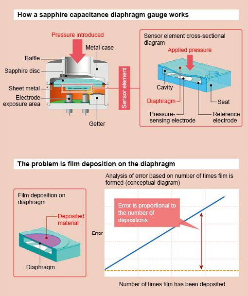
Semiconductor manufacturing requires a vacuum gauge with high resistance to corrosive gases and heat influence from chambers, and Azbil responded to these needs in 2006 with the appearance of its SPG Series sapphire capacitance diaphragm gauges. SPG gauges use a very thin artificially grown sapphire diaphragm that deforms slightly according to the level of vacuum. By measuring the capacitance change of the diaphragm, which also changes in proportion to the vacuum, these gauges achieve a high degree of accuracy and reliability even under severe process conditions.
Recent years have seen the increasing use of a semiconductor manufacturing process called atomic layer deposition (ALD), in which a semiconductor wafer is overlaid with an exceedingly thin yet comprehensively covering layer of a different material. This technology has made it possible to increase the speed and the size of integrated circuits, such as CPUs and memory devices.
ALD has many advantages, but the raw material of the film is deposited in the chamber inside the semiconductor manufacturing equipment, which includes vacuum gauges, and while the film forms, the level of vacuum inside the chamber must be accurately controlled and maintained. If film is deposited on the vacuum gauge that is measuring the internal level of vacuum, it will cause an error in the measurement results.
Key Innovations
By combining three technological innovations, this problem with ALD was resolved
Azbil has developed a sapphire capacitance diaphragm gauge for atomic layer deposition based on its sapphire capacitance diaphragm gauge, which became available in 2006. With the development of three technologies — a new diaphragm structure, a method of controlling the area of deposition, and suppression of deposition — Azbil has succeeded in dramatically reducing measurement error due to deposition.
- New Diaphragm Structure
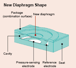
In ALD, reducing the deposition of film in the vacuum gauge to zero is, in principle, not feasible. Even with a sapphire capacitance diaphragm gauge, if base material is deposited on the diaphragm, the diaphragm’s thermal expansion coefficient will change, causing the diaphragm to remain in a deformed state, leading to deviation of the “zero point” for measurement.
To handle this problem, a unique shape was created by slightly thinning the center part of the diaphragm, such that the diaphragm’s degree of deflection does not change even if film is deposited. The concept is to offset the deflection of the thin part with that of the thick part to reduce error. Success was achieved in determining an optimal shape through deformation simulation and testing.
- Controlled Area of Deposition
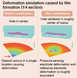
Depending on the material used, film may not be deposited evenly on the diaphragm. In this case, even with the newly developed diaphragm structure, the diaphragm will not deflect uniformly, leading potentially to deviation of the zero point. Since the deposition of a uniform film cannot be anticipated, conversely, Azbil devised a method whereby error in the sensor output is reduced even while the diaphragm is deflected by intentionally causing deposition in a specific location.
In the sensor, there is a pressure-sensing electrode that measures the pressure as well as a reference electrode that corrects for the effect of temperature. Film is deposited at a point in roughly the center of the diaphragm radius where it
covers both the pressure-sensing electrode and the reference electrode. Specifically, there is a very small hole at a location corresponding to the sapphire disc that covers the diaphragm to draw in the gas that causes deposition. - Dramatic Suppression of Deposition
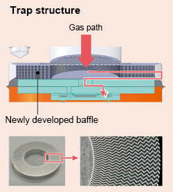
Even with these two countermeasures, there is no change in deposition (depending on the film material). It was anticipated that this would cause a loss of measurement sensitivity and measurement accuracy over time. Therefore, a trap (baffle), which is a very fine filter that removes the base material for the film, was developed to suppress deposition to the greatest extent possible. The structure of this trap includes as many as 4000 fine paths on the circumference to ensure responsiveness. By including this trap structure, the amount of deposition on the diaphragm was calculated to be reduced to 0.03 %, ensuring long-term stability.
Results and Future Outlook
High accuracy and high stability in severe environments, and continuing improvement in response to user needs
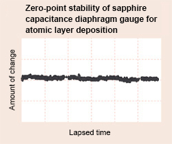
The sapphire capacitance diaphragm gauge has evolved into a sapphire capacitance diaphragm gauge for atomic layer deposition. This latter vacuum gauge is equipped with several outstanding characteristics, such as very little shift in the zero point even if film is deposited, as well as long-term stability. The gauge continues to receive high praise from our customers, who say they feel confident using Azbil-made vacuum gauges developed in Japan. Having successfully implemented a resolution for a problem in the latest manufacturing process, we look forward to continually meeting the challenge of solving the problems faced by customers at their worksites.
*Handling of products and services described in “azbil techne” may differ by country or region.
- Azbil Corporation Info
- Corporate Philosophy / Symbol / Policies
- azbil Group Corporate Social Responsibility
- Investor Relations
- Digital Transformation (DX)
- Medium-term Plan
- Research & Development
- Production
- Safety and Dependability of Products and Services
- Procurement
- Exhibitions & Seminars
- Public Relations
- azbil Group
- Certifications
- Global Network